
PFC Design – Maximizing Efficiency and Lowering Cost with GaN Transistors
GaN Systems releases industry’s first E-HEMT bridgeless-totem-pole Power Factor Correction reference design
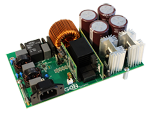
OTTAWA, Ontario, May 9, 2017 – Achieving efficiencies greater than 98% in conventional Power Factor Correction (PFC) circuits is challenging. The major hurdle is fixed diode bridge losses. An option to overcome this is to use silicon MOSFETs in place of the diodes to achieve efficiencies of 99% or more. However, this BTPPFC approach suffers from poor reverse recovery performance, is suitable only for low power, and requires complicated control parameters. GaN Systems mitigates these drawbacks by replacing silicon MOSFETs with GaN E-HEMTs that eliminate the body diode (zero Qrr) and exhibit very fast switching. To provide design engineers with a platform to demonstrate the performance of GaN HEMTs, GaN Systems has released the GS665BTP-REF, the industry’s first 3 kW continuous current mode (CCM) E-HEMT-based BTPPFC reference design.
The 3 kW GS665BTP-REF reference design compares the switch-on losses of a silicon-based CoolMOS CFD2 with losses exhibited by a GaN Systems 650 V E-HEMT. The results show that GaN has superior reverse recovery. Operating the CCM BTPPFC at 50 kHz, GaN dissipates only 0.75 W switching loss due to the Qoss Loss at turn-on, while the CoolMOS CFD2 shows a loss of 20 W, solely due to Qrr. The result is excellent hard-switching performance in a CCM BTPPFC with maximized efficiency.
Comprehensive documentation for the GS665BTP-REF reference design, entitled “High-Efficiency CCM Bridgeless Totem Pole PFC Design using GaN E-HEMT,” is available for download from GaN Systems website. The documentation includes the motivation, operating principles, and design considerations for the BTPPFC using 650 V GaN E-HEMTs. Also included in the documentation are discussions pertaining to test setup, test results (i.e. efficiency, power factor, waveforms, thermal measurements), and applications.
Paul Wiener, GaN Systems VP of Strategic Marketing, commented on the release of the reference design, “Now power design engineers have a tool to help them leverage the increased efficiencies and reductions of space, weight and BOM costs provided by GaN transistors. Today we are seeing these benefits show up in products as diverse as battery chargers, energy storage systems and power supplies in enterprise applications. As design engineers explore ways to improve power system performance, we expect that this reference design will play an instrumental role in the development of many more commercial products.”