GaN Systems teams with the UK EPSRC Power Electronics Centre to accelerate the use of high speed GaN transistors in future power conversion or control applications Nottingham, England – At a ceremony held at the EPSRC Centre for Power Electronics Annual Conference 2016 in Nottingham, England, a post-graduate team from Imperial College London received the…
https://gansystems.com/wp-content/uploads/2016/08/press-icon-3.jpg126200LiquidWebhttps://gansystems.com/wp-content/uploads/2024/03/infineon-formerly-gan-fc-2.pngLiquidWeb2016-08-04 07:03:372023-06-20 08:11:22Imperial College London Wins GaN Systems Geoff Haynes Future Power Challenge
At APEC 2016 it became abundantly clear to the industry that GaN transistors are here, they’re now, and they’re proliferating. GaN Systems, EPC, Transphorm, Panasonic, Infineon, Texas Instruments, and other manufacturers and developers all displayed GaN products in varying readiness, from existing only on PowerPoint slides to actual customer production units. It’s been fascinating to watch…
https://gansystems.com/wp-content/uploads/2016/07/h-slider-img-1-1.jpg244322LiquidWebhttps://gansystems.com/wp-content/uploads/2024/03/infineon-formerly-gan-fc-2.pngLiquidWeb2016-08-04 06:52:182023-06-20 08:11:05Integration or Optimization…Which Comes First?
EDN describes how GaN is outperforming silicon in power management applications. This article describes how GaN transistors enabled CE+T’s Red Electrical Devils team to design the tour de force inverter that won Google’s Little Box Challenge. Their inverter produced a power density of 143 W/cubic inch in 14 cubic inches, outperforming the Little Box Challenge…
https://gansystems.com/wp-content/uploads/2016/08/littlebox.jpg90200LiquidWebhttps://gansystems.com/wp-content/uploads/2024/03/infineon-formerly-gan-fc-2.pngLiquidWeb2016-08-04 06:49:512023-08-08 09:00:54Google Little Box Challenge Showcases GaN Power Element
Over the years, GaN power has been sarcastically described as “the technology of the future…and always will be.” While silicon carbide devices have been gaining a stronger beachhead in displacing IGBTs in higher voltage applications, the evolution of GaN as a cost-effective alternative to Si MOSFETs in applications from 200V up through 600V was, in…
https://gansystems.com/wp-content/uploads/2016/07/bodos-power.jpg72200LiquidWebhttps://gansystems.com/wp-content/uploads/2024/03/infineon-formerly-gan-fc-2.pngLiquidWeb2016-07-28 14:31:442023-06-20 08:11:21Podium Session at PCIM Europe Marks New Chapter in GaN Power Device Adoption
GaN Systems’ Di Chen explains how to test 650 V GaN transistors for your application. Our eval board is easily configured into any half-bridge-based topology, including synchronous boost and buck conversion modes, as well as pulsed switching to evaluate transistor waveforms.
https://gansystems.com/wp-content/uploads/2020/04/gs66508t-evbhb-650-v-half-bridge-evaluation-board.jpg356634LaunchSnaphttps://gansystems.com/wp-content/uploads/2024/03/infineon-formerly-gan-fc-2.pngLaunchSnap2016-06-13 13:27:142023-07-14 14:23:27Getting started with the GS66508T-EVBHB 650 V half bridge evaluation board
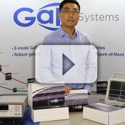
That GaN transistors outperform silicon-based solutions has never been more convincingly demonstrated than by CE+T’s Red Electrical Devils, who won first place in Google’s Little Box Challenge. At APEC 2016, Girvan Patterson, President of GaN Systems, describes to Design World / EEWorld’s Lee Teschler CE+T’s winning design of an uber-compact inverter using GaN transistors. The…
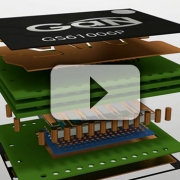
GaNpx packaging provides extreme speed and current with: 1) a near chipscale embedded package, 2) high current density & low profile, 3) optimal thermal performance, 4) extremely low inductance, and 5) no wirebonds. GaN Systems makes it easy for designers and systems engineers to adopt gallium nitride solutions.
https://gansystems.com/wp-content/uploads/2020/04/gan-systems-ganpx-packaging-process-flow.jpg356634LaunchSnaphttps://gansystems.com/wp-content/uploads/2024/03/infineon-formerly-gan-fc-2.pngLaunchSnap2016-04-13 13:32:402023-07-14 14:20:44GaN Systems – GaNpx Packaging Process Flow
The island structure is the core GaN Systems IP. It has the dual advantage of an up to four times reduction in the size and cost of gallium nitride devices, while transferring substantial current from the on-chip metal to a separate carrier. GaN Systems makes it easy for designers and systems engineers to adopt gallium…
https://gansystems.com/wp-content/uploads/2020/04/gan-island-technology.jpg356634LaunchSnaphttps://gansystems.com/wp-content/uploads/2024/03/infineon-formerly-gan-fc-2.pngLaunchSnap2016-04-13 13:32:382023-07-14 14:19:59GaN Systems – Island Technology
Gallium nitride transistors increase efficiency, lower power consumption and reduce system size and weight. GaN Systems is the first place system designers go to realize those benefits.