Gallium Nitride Sets Innovation Bars Higher
The following article, written by Mathew Dirjish, originally appeared in Sensors Online.
Silicon has been the mainstay of semiconductor fabrication for as long as one can remember. It is the meat of transistors, OP amps, microprocessors, MCUs, PLCs, and numerous other devices. The material has proven more than viable and reliable and will be with us for countless years ahead.
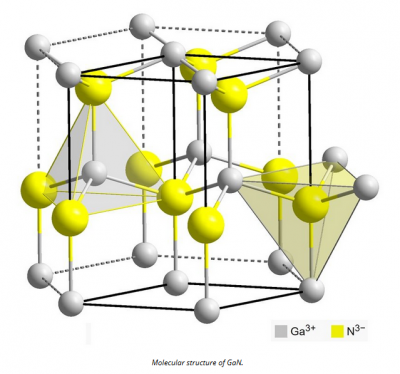
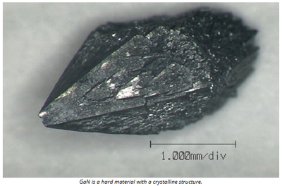
Starting with power devices, a not so new kid on the block is proving to be silicon’s competitor to be reckoned with. Gallium nitride (GaN) is a semiconductor commonly used in light-emitting diodes. It is a hard material with a crystal structure, a property that makes it desirable for use in opto applications and high-power devices.

To make a long technical story shorter, the material has proven itself in fabricating power devices. Certain sources indicate that the first enhancement-mode gallium nitride transistors became available in 2010.

Designed to replace power MOSFETs in applications where switching speed or power conversion efficiency is critical, the GaN transistors exhibit significant advantages over silicon MOSFETs, particularly in the cost versus performance challenges.
Now, it appears GaN is making inroads to the world of sensors. It stands to reason since many sensors are silicon based and with the emerging need for multiple sensors on a chip, a.k.a., sensor fusion, GaN could open up many new areas for sensor innovation. The possibility of combining power functions, sensors, and optical functions on a small device may not be too far away in the future.
To get the best insight into this material and what we can see in the future, I had a brief Q&A with Jim Witham, the CEO of GaN Systems. The company manufactures a range of gallium nitride high power transistors for consumer, enterprise, industrial, solar/wind/smart-grid, and transportation power-conversion applications. The devices boast exceptionally low on-resistance, negligible charge storage, and enable switching efficiencies in excess of current silicon devices.
Mat Dirjish (MD): GaN Systems focuses on the use of gallium nitride instead of silicon in the development of power semiconductors. For some of our readers who may not be aware of the benefits of GaN and the tradeoffs of silicon, what sets the use of GaN above silicon for power applications?
Jim Witham (JW): By replacing legacy components with GaN transistors, engineers can design electronic systems that are 4x smaller, 4x lighter, that exhibit 4x less energy loss, and are less costly. The performance advantages provide customers with a profound array of benefits across markets from the IoT and datacenter servers to industrial equipment, electric vehicles (EVs), and autonomous vehicles.
MD: Although the primary focus appears to be transistors, HEMTs in particular, GaN-based violet laser diodes are used in Blu-Ray disc players. Do you foresee GaN being viable for other semiconductor types and if so, what is possible?
JW: The three major applications for GaN are LED, power, and RF. GaN Systems focuses on power. The fourth application showing great potential is GaN sensors.
MD: Is GaN easily substituted for silicon in general semiconductor design/manufacturing? What are the major challenges in making the switch?
JW: In general, yes, one can think of our GaN transistors as just extremely fast MOSFETs. Second, we have solved the design challenges for customers by making our transistors easy to use and providing the design tools engineers expect. Evaluation kits, discrete parts and reference designs are easily acquired through common sales channels. Datasheets, application notes, and solution design files are available with an easy click from our website.
MD: Several sensor types are implemented on silicon and sensor fusion, the combination of two or more sensor types on a single chip, relies on silicon. Is GaN a viable material for creating low-power, fast reacting sensors and multiple sensor integrations?
JW: GaN sensors are receiving a lot of attention and focus today. Mercury detection, pH analysis, hydrogen sensing, and DNA and protein sensing are just a few of the areas being researched with GaN HEMT materials. As mentioned above, this could emerge as the fourth, very large application for GaN.
MD: In July, BMW’s investment arm, BMW i Ventures, made a significant investment in GaN Systems, which is viewed as a major display of confidence in the technology. What are some of the projects GaN will be working on as a result of this investment?
JW: As we recently announced, GaN Systems will use the funds to expand our global sales efforts and to accelerate new product development. The products under development will be used to help engineers design more efficient electronic systems in the markets we target, which include consumer, datacenter, industrial and transportation applications.
MD: What types of emerging applications are offering growth potential for GaN devices? Obviously there will be greater demands for power devices in IoT and IIoT systems. What impact will areas such as energy harvesting, artificial intelligence, augmented reality, and virtual reality on the direction of GaN devices?
JW: The IoT and IIoT segments, and I would add 5G to those, are very exciting. These applications generate massive amounts of data, driving the need for increased data storage and processing, which requires more power supplies and servers. GaN devices reduce power consumption and increase power supply density, saving customers operating costs and allowing more servers in the same rack. The same holds true for the automotive ADAS and autonomously driven vehicle space where automotive manufacturers are building datacenters to manage the 10X explosion in data generated by these vehicles. EV and HEV systems are undergoing extensive electrification, which increases semiconductor demand 3x to 4x more than vehicles currently require.
Wireless power transfer is an emerging application with a direct tie to sensors. This is a perfect method to supply power to these sensing devices. Then there are robot and drone applications that are just starting to take off; these will also leverage the advantages of wireless power transfer and charging.
Another emerging application for GaN is artificial intelligence and machine learning. These applications use microprocessors, GPUs and memory in their high-performance computing (HPC) that require higher power, in the order of 500 W in the same volume that currently delivers only 200 W. GaN transistors provide a path for designers to increase power density without adding volume or weight.
MD: If you can speak about it, what developments does GaN Systems have on the drawing board for the future?
JW: Our plans include product expansion in several different vectors – voltage, current, and frequency performance. Additionally, we will integrate features to save customers more space, cost and time.
In summary, GaN is undoubtedly going to make more than a little noise in several markets, particularly the sensors markets while continuing to make great strides in the power sector. It is definitely a technology to keep a steady eye on.


