
Gallium Nitride is Moving Forward
The following article was written by Achim Scharf and published in the November 2016 issue of Power Electronics Europe.
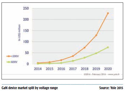
According to market researcher Yole 2015 – 2016 have been exciting years for the GaN power business – 600V GaN is today commercially available, after many ups and downs. And GaN power ICs have debuted, opening new market perspectives for GaN companies. GaN power business is expected to reach $280 million in 2021, with an 86 % compound annual growth rate (CAGR) between 2015 and 2021. The market is driving by emerging applications including power supply for datacenter and telecom, AC fast charger, automotive LiDAR, Envelope Tracking, and wireless power.
“In the digital arena Moore’s law – doubling the transistor count on chip every 18 month – has now been broken, but in power electronics we are just in the beginning with the role of GaN”, EPC’s CEO Alex Lidow points out. “GaN is the logical technological successor to Silicon for power conversion and analog devices, and possibly also for digital components as well. We are away by the factor of 800 of the theoretical GaN limits, this technology is able to be integrated up to the level of NMOS.
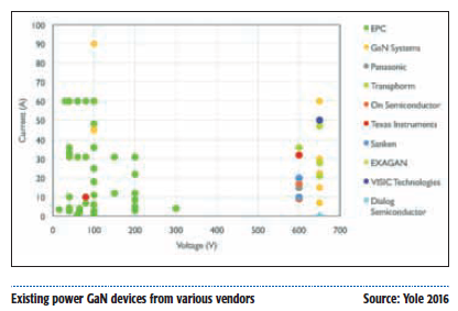
“Numerous powerful developments and key collaborations have been announced during the last years – a promising and fast-growing industry”, comments Hong Lin, Technology & Market Analyst at Yole (www.yole.fr). To mention are Integrated Device Technology (www.IDT.com), Efficient Power Conversion (www.EPC-co.com), Infineon Technologies (www.Infineon.com) and Panasonic (https://eu.industrial.panasonic.com/), Exagan (www.exagan.com) and German Xfab (www.xfab.com), TSMC (www.tsmc.com) and GaN Systems (www.gansystems.com). TSMC is the first company to offer both 100 V and 650 V GaN foundry service in a 6-inch fab. The idea of bringing GaN from the power semiconductor market to the much bigger analog IC market is of interest of several other players too. For example, EPC and GaN Systems are both working on a more integrated solution. In parallel Texas Instruments (www.ti.com) announced a 80 V power stage in 2015 and a 600V power stage in 2016. Fast-forward to 2016 end users can now buy not only low-voltage GaN (<200 V) devices from EPC, but also high voltage (600V/650V) components from several players, including Transphorm (www.transphormusa.com), GaN Systems, and Infineon/Panasonic.
And Visic (www.visic-tech.com) announced in September 2016 a 1200 V power module. Based in Nes Ziona, Israel, VisIC Technologies, Ltd. was established in 2010 by experts in GaN technology. The GaN module have typical on-resistance down to 0.04 Ω. Target applications are power converters for motor drives, three-phase power supplies and other applications requiring current switching up to 50A. “This technology supports reduced gate charge and capacitances without losing the benefits of low RDS(ON), offering an ultra-low maximum switching energy down to 140 ?J. Switching losses are three to five times lower compared to SIC MOSFETs”, said CTO Gregory Bunin. Also in September the company launched a new 12 A GaN switch in a smaller bottom-side cooled package with an on-resistance of 0.080 Ω.
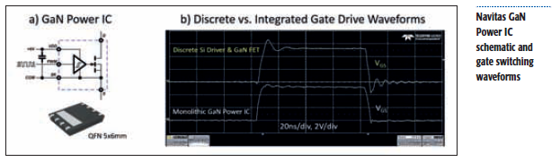
A new start-up, Navitas Semiconductor (www.navitassemi.com), announced their 650 V GaN power IC based on Hughes Lab technology (www.hrl.com) at APEC in March 2016 and later in Europe at PCIM 2016. “GaN is ready for the market and we are integrating things which have not been integrated before”, CTO Dan Kinzer stated. The company has designed a fully integrated GaN IC with integrated gate drive in QFN 5 mm x 6 mm package. “This e-mode device features 20 times lower drive loss than Silicon, the driver impedance is matched to the power stage. Also almost zero inductance leads to low switching losses – and our 650-V process allows switching frequencies of up to 27 and 40 MHz! The switch is not the limit, it is the magnetics”. According to Kinzer this device can also be used as a 500-V synchronous rectifier.
AllGaN™ is the first platform which allows monolithic integration of 650 V GaN IC circuits (drive, logic) with GaN FETs. This ‘GaN Power IC‘ contains features such as hysteretic input, voltage regulation and ESD protection – all integrated in the same GaN layer as the main power device. This monolithic integration of drive and switch is impractical using d-mode GaN, vertical GaN or SiC Lateral ‘GaN-on-Si‘ construction means immediate high volume capability using existing foundry processes. Within the AllGaN solution, the GaN FET gate is driven safely, precisely and efficiently by the upstream integrated GaN driver. Standard 3.3 V, 5 V or 15 V PWM signals are fed directly into the GaN Power IC for an easy, low component count design. Integrating the driver also reduces ringing and enables tight control of turn-on, turnoff for high-frequency half-bridge applications.
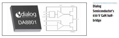
Dialog Semiconductor plc (www.dialogsemiconductor. com) announced end of August its first GaN power IC product offering, using TSMC’s 650 V GaN-on-Silicon process technology. “The exceptional performance of GaN transistors allows customers to deliver more efficient and compact power adapter designs that meet today’s market demands,” said Mark Tyndall, SVP Corporate Development and Strategy, Dialog Semiconductor. “GaN technology offers the world’s fastest transistors, which are the core of high-frequency and ultra-efficient power conversion. Our DA8801 half-bridge integrates building blocks, such as gate drives and level shifting circuits, with 650 V power switches to deliver an optimized solution that reduces power losses by up to 50 %, with up to 94 % power efficiency. The product allows for a seamless implementation of GaN, avoiding complex circuitry, needed to drive discrete GaN power switches. The new technology allows a reduction in the size of power electronics by up to 50 percent, enabling a typical 45 W adapter design today to fit into a 25 W or smaller form factor. This reduction in size will enable true universal chargers for mobile devices.”
What the industry expects from GaN expressed Thomas Heckel from Fraunhofer IISB (www.iisb.fraunhofer.de) in Erlangen earlier this year at the CIPS conference: ”We expect a normally off characteristic, better performance than Si and even SiC, and more vendors”. At IISB a test system has been set up for the evaluation of various GaN transistors. A 200-V transistor switched at 100 V exhibited dynamic on-resistance (120 mΩ to 80 mΩ) which was not specified in the datasheet; a 650 V/150 mΩ cascode was opened which needs external gate resistor, this type exhibited poor controllability; a 650 V/45 mΩ with four GaN transistors showed better controllability – but is commercially not more available; a 650 V/50 mΩ normally-off device had better dynamic on-resistance but reached not the datasheet specifications. Only Panasonic’s 600 V GIT device exhibited no dynamic on-resistance!
International Rectifier was the first to introduce a cascoded GaN transistor and was acquired by Infineon for $3 billion due to its GaN leadership in late 2014. Meanwhile the cascode topology has been skipped and by licensing the Panasonic GIT an e-mode technology will be favored by Infineon. This turn obviously marks an industry change to support emode or normally-off devices in the future.
New application possibilities
“GaN technology is disruptive, in the best sense of the word, making possible what was once thought to be impossible”, comments EPC CEO Alex Lidow. GaN technology is 10 times faster, significantly smaller, and with higher performance at costs comparable to Silicon-based MOSFETs. The inevitability of GaN displacing the aging power MOSFET is becoming clearer with domination of most existing applications and enabling new ones”.
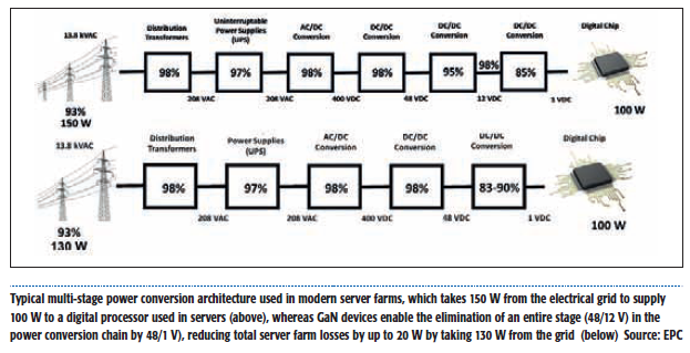
The explosion of digital content, big data, e-commerce, and Internet traffic is also making data centers one of the fastest-growing consumers of electricity in developed countries, and one of the key drivers in the construction of new power plants. In 2014, data centers (in the US) consumed about 100 billion kWh of energy and it is projected by the Natural Resources Defense Council (www.nrdc.org) that data center electricity consumption will increase to roughly 140 billion kWh annually by 2020, the equivalent annual output of 50 power plants. The power needed to support this rapidly growing demand comes from the electrical grid, and goes through multiple conversion stages before it actually feeds the remaining energy into a digital semiconductor chip. The losses due to the transmission and multiple conversion stages of electricity – from the power plant to the computer chip, shows that the power grid needs to supply 150 W to meet the demands of a digital chip that may need only 100 W of power. Thus the combined waste across the US due to power conversion for servers is 33 billion kWh, equivalent to almost a dozen power plants. But the overall wasted energy within the server farm is even more, because every watt of power loss through power conversion is actually energy that is converted into heat, and removing this heat demands even more power.
Since the adoption of the 12 V intermediate bus architecture (IBA), bus converters are currently approaching about an order of magnitude increase in output power, from around 100 W to current designs of around 1 kW in a quarter brick footprint. This means that the amount of current on the 12 V bus to the POL converters has also increased by a factor of 10 and, without reductions in busing resistance, a two order of magnitude increase in busing conduction losses follows. GaN-based solutions have already demonstrated significant efficiency improvements compared to Silicon based solutions in conventional IBA systems. However, with the increasing conversion losses in the 48 V input bus converter, the mounting 12 V busing losses on the motherboards, and the higher performance of GaN technology, different architectures may now be considered, such as going directly from 48 V input to load using non-isolated POL converters. For the 48 V input, an 80 V eGaN monolithic half-bridge IC (EPC2105), embedded in an EPC9041 demonstration board, was selected for the much higher stepdown ratio. “The direct savings by eliminating just the last stage in the server farm power architecture is not only a cost reduction, but also a reduction of power consumed between 7-15% depending on the GaN-based approach. This correlates to direct savings of up to 21 billion kWh per year when compared with Silicon-based solutions. This savings is increased further when air conditioning energy costs inside the server farm are added, bringing the total to almost 25 % of the 140 billion kWh consumed by servers in the US alone”, Lidow calculated.
The 48 V power architecture is getting more attention since Google (www.google.com) has joined the Open Compute Project (www.opencompute.org) in early 2016. OCP will help to drive standardization in IT infrastructure. More specifically, Google will contribute a new rack specification that includes 48 V power distribution and a new form factor to allow OCP racks to fit into data centers. “Energy efficiency in computing is a topic that has been near and dear to our hearts since the early days. We began advocating for efficient power supplies in 2003, and in 2006 shared details of our 12 V architecture for racks inside our data centers – the infrastructure that supports and powers rows upon rows of our servers. In 2009, we started evaluating alternatives to our 12 V power designs that could drive better system efficiency and performance as our fleet demanded more power to support new high-performance computing products, such as high-power CPUs and GPUs. We kicked-off the development of 48 V rack power distribution in 2010, as we found it was at least 30 % more energy efficient and more cost effective in supporting these higher performance systems. Our 48 V architecture has since evolved and includes servers with 48V to POL designs, and rack- level 48 V Li-Ion UPS systems. Google has been designing and using 48V infrastructure at scale for several years, and we feel comfortable with the robustness of the design and its reliability. As the industry’s working to solve these same problems and dealing with higher-power workloads, such as GPUs for machine learning, it makes sense to standardize this new design by working with OCP. We believe this will help everyone adopt this next generation power architecture”, commented Google’s Technical Program Manager John Zipfel.
Another example – the automotive industry understands the trend to have the interior of the car a “living space” and has begun to show its vision of the future for the fully mobile lifestyle. The dashboard is being taken over by the smartphone, while sensors and computers are being added to increase its safety. Moving toward a longer-term goal, vehicles are on a path to become fully electric, reducing fossil fuel usage.
A rapidly emerging technology to enable the batteries in our electronic devices keep up with the demands added by the vehicle’s infotainment system is wireless power transfer. The latest techniques enable wireless charging of multiple objects without contact with the power transmission unit (PTU) with efficiencies similar to wired chargers. Wireless phone charging in a car is becoming more critical as the smartphone itself is becoming the information receiver and router for the dashboard infotainment center.
Several automotive manufacturers are adopting operating system standards that enable seamless interfaces to dashboards that become “slaves” to the information and entertainment available in the drivers and other occupants’ smartphones.
The AirFuel Alliance (www.airfuel.org) wireless power transmission standard developed by a consortium of electronics industry leaders such as Samsung, Qualcomm, Intel, and EPC is undergoing rapid adoption in mobile phone and tablet charging applications. To implement this standard, several automotive manufacturers are developing embedded wireless charging stations in the center console of the vehicle so smartphones, as well as other mobile devices, can remain charged while the automobile is in operation, despite intense and continuous usage. Given that the AirFuel Alliance standard uses a 6.78 MHz standard frequency for power transmission, a stretch for Silicon power devices, GaN technology is the heavy favorite for adoption in both mobile and automotive applications.
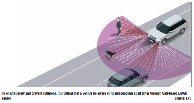
In addition to wireless charging becoming commonplace within the car’s cabin, it is becoming available to charge fully electric cars or plug-in hybrids. With a “charging mat” as the power transmitter, one will merely have to place the mat on the floor of your garage and park the car over the mat without the need to “connect the car to an outlet.” To ensure safety and prevent collisions, it is critical that a vehicle be aware of its surroundings at all times. The higher the speed of the vehicle, the more rapidly the “situational awareness” system needs to sense, and the more precisely it needs to interpret the distance to the potential hazard.
Today automotive manufacturers use a variety of sensors in these safety-related functions, including ultrasonic sensing, microwave radar short-range radar, and video pattern recognition. Light Distancing and Ranging (LiDAR) sensors have recently begun to emerge in automotive sensing applications. Although Lidow anticipates broad adoption in automotive, initially LiDAR sensors were used to generate three-dimensional digital topographical maps used for landscape mapping and navigation software. Because LiDAR chases the speed of light for improving resolution, GaN power transistors, with about a 10 times advantage in switching speed, GaN FETs have been used almost exclusively in these mobile applications. “The imaging speed and depth resolution has become so good using eGaN FETs that manufacturers experimenting with autonomous vehicles are using similar LiDAR sensors for driverless navigation systems. In addition, several automakers are incorporating eGaN FET-based LiDAR sensors in their vehicles for general collision avoidance and blind spot detection. LiDAR has a very exciting future, since it is the detection and guidance system being used for driverless cars”, Lidow stated.
Also the evolution – from an internal combustion engine, to hybrid vehicles, plug-in hybrids, and, finally, to fully electrically powered cars – is potentially a very large market for GaN technology. The demand for electrical power grows in proportion to the amount of propulsion handled by the electric motor; according to Tesla (www.tesla.com) the model S delivers 310 kW of electrical power to the rear wheels. Delivering more power to propel a vehicle requires higher voltages in order to keep the current levels flowing through the motor windings with minimum conduction losses. Today the dominant transistor in electric or hybrid vehicle propulsion systems is the IGBT in voltages from 500 to 1200 V. “However, wide bandgap transistors made using either SiC or GaN technology hold great promise for this high power application, since they have higher efficiency at lower switching frequencies and possess the ability to operate at much higher temperatures. The requirements for electric motor drives sit at the interface between GaN, SiC and IGBT technologies. Ultimately, the cost and reliability of the electric drive system will determine the winner for this application, but for now, it is too soon to call”, Lidow expects. “In the future, as electric vehicles gain acceptance and become more ubiquitous, motor controls for the powertrain has the potential to become an enormous market for GaN transistors. The issue among the competing technologies – GaN, SiC and IGBT – will be the cost. The automotive industry is undergoing a technological disruption and is taking advantage of high performance gallium nitride technology. GaN devices are appearing in an ever-increasing number of systems, with the future looking even more promising. Several areas are clearly emerging, as discussed above.
As a practical example a design methodology of a 50 W isolated DC/DC converter based on EPC’s 200 V GaN transistors serving as a power supply for aircraft equipment has been awarded as Best Paper of PCIM Europe 2016. The particularity of this work is the design of a full converter regarding two antagonistic requirements which are a wide input voltage and high efficiency. In high frequency applications, it seems clear that using GaN transistor creates a real improvement of the efficiency due to its low output charge. In a soft-switching topology the device output charge has an important impact on the energy required to achieve ZVS condition providing a larger power storage and transfer period means naturally a higher efficiency. The other GaN transistor benefits are its low total gate charge and its low drain to source on-state resistance, reducing the drive power (losses) and conduction losses respectively. All these features are implemented in a smaller packaging with less parasitic inductances compared to a Si MOSFET with similar power characteristics. The efficiency approaches 92 % at the nominal input voltage (28 V) and the peak efficiency is 95.5 % for an input voltage of 18 V.
Certainly the most impressive design in the higher voltage range based on GaN System’s devices (GS66508P e-mode GaN power transistor) was the winning design of Google’s Little Box Challenge early this year. The Little Box Challenge was a design contest presented by Google and the IEEE Power Electronics Society to spur innovation in power inverter design with the highest power density (at least 50 Watts per cubic inch) and an efficiency of >95 % with a $1,000,000 prize. According to Google inverters will become increasingly important to economy and environment as solar PV, batteries, and similar power sources continue their rapid growth. The innovations inspired by this prize will have wide applicability across these areas, increasing efficiency, driving down costs, and opening up new uses cases that we can’t imagine today. It also doesn’t hurt that many of these improvements could make data centers run more safely and efficiently.
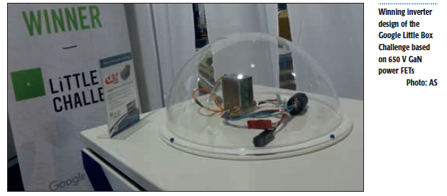
Google and the IEEE Power Electronics Society awarded the $1 million prize to Belgium’s CE+T’s Red Electrical Devils for designing, building and demonstrating an inverter with the highest power density and smallest volume. The key goal of the challenge was to reach an inverter power density in excess of 50 W/cubic inch in a volume of under 40 cubic inches – a feat which had never been done before. Their winning inverter design produced a power density of 143 W/cubic inch in 14 cubic inches, outperforming the Little Box Challenge power density goal by nearly a factor of 3 thanks to GaN power, which, according to Google, “is 10 times more compact than commercially available inverters”.
Emerging market
Despite these developments, the GaN power market remains small compared to the gigantic $335 billion Silicon semiconductor market. According to Yole’s investigation, the GaN power business was less than $10 million in 2015. “But before you think twice about GaN, remember that a small market size is not unusual for products just appearing on the market”, comments Lin. Indeed first GaN devices were not commercially available until 2010. According to Yole’s analysts, the most important point to be noticed is the potential of GaN power. Indeed they expect the GaN power business to grow, reaching a market size of around $300 million in 2021 at a 2016 – 2021 CAGR of 86 %. “The current GaN power market is mainly dominated by low voltage (<200 V) devices, but the +600 V devices should take off”, comments Zhen Zong, Technology & Market Analyst at Yole.
More than 200 patent applicants are involved in the power GaN industry, stated KnowMade (www.knowmade.com) in its GaN for Power Electronics: Patent Investigation report in August 2015. Such figure is showing the strong interest from power players in the GaN business. The take-off of patenting activity took place in the 2000s with a first wave of patent publications over the 2005-2009 period mainly due to American and Japanese companies. A second wave started in 2010 while first commercial GaN products, collaborations and mergers and acquisitions emerged. “In the today’s power GaN market, it is crucial to understand the global patent landscape thorough in-depth analyses. This approach helps the companies to anticipate the changes, identify and evaluate business opportunities, mitigate risks and make strategic choices. “comments Nicolas Baron, CEO of KnowMade. “The time evolution of patent filings has reached a peak, and we expect a slowing down of new patent applications. Meanwhile, granted patents worldwide should increase after successful prosecution of the numerous pending patent applications. We believe the second peak of patent filings combined with the significant ratio of patents in force and the large number of patent applications still in the pipeline worldwide is an indication of the technology maturity heralding a future ramp-up of the GaN power market”, he added.
- Literature
Power GaN 2016 report, Yole Developpement
Breakthrough for GaN Power ICs, Power Electronics Europe May 2016, page 12
APEC 2016, Power Electronics Europe May 2016, page 20-23
CIPS 2016, Power Electronics Europe May 2016, page 17
GaN Matures…, Power Electronics Europe May 2016, page 26-28
Optimizing GaN Performance…, Power Electronics Europe May 2016, page 29-31
PCIM 2016, Power Electronics Europe June 2016, page 9-15
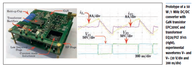
1 MHz Converter with 95 % Peak Efficiency…, Power Electronics Europe June 2016, page 16-18