
Using simulation to optimize GaN-powered designs
Comparisons of transistor device models and simulation techniques illustrate which approach works best for specific design scenarios.
This article, written by Lei Kou and Lucas Lu, was originally published on Power Electronics Tips, October 27, 2021. Read the full article here.
When designing a new system based on Gallium Nitride (GaN) power transistors, simulation provides engineers with a powerful design optimization tool. Through simulation, designers can estimate system efficiency, choose the appropriate device or topology, find suitable thermal strategies, and optimize the magnetics design. Once the design is complete, simulation also aids in system debugging.
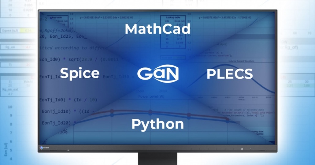
There are three types of GaN transistor modeling in wide use: SPICE (Simulation Program with Integrated Circuit Emphasis), Analytical Loss Modeling, and PLECS (Piecewise Linear Electronic Circuit Simulation). Similarly, there are three widely used system-level simulation techniques: PLECS, Python, and Mathcad. Comparisons of transistor device models and examples of simulations offer a detailed focus on the different approaches.
When designing a GaN-powered product or system, good simulation tools are essential for fast time-to-market. For instance, a loss breakdown analysis helps the designer verify the system efficiency and make modifications before building hardware. It also enables the selection of the most suitable transistor device characteristics and the best topology. For example, results showing the conduction loss of the system dominates will guide the designers toward using a lower RDS(on) transistor.
By determining the system loss results through simulation, the user can settle on thermal design that realizes the system design targets. Simulation can also help optimize the magnetics and the choice of the switching frequency. Similarly, simulation reveals the system’s maximum efficiency point, how high the current can go under certain conditions, as well as the maximum operating rating.
Learn how to maximize system performance with GaN Systems simulation tools. Watch our webinar, “Using Simulation to Maximize GaN Powered Design,” when you click here.
GaN transistor device modeling
Different GaN device models can be used depending on the design topology and critical design parameters. The commonly used SPICE model allows designers to evaluate and observe GaN switching parameters: rise time (Tr), fall time (Tf), dv/dt, EON/EOFF; gate driving performance: gate waveform and the influence of RG on switching, and thermal performance under different conditions like transient and steady state.
The architecture of the GaN transistor spice model resembles that of a silicon transistor. The GaN Systems SPICE Model, for instance, shows good correlation with actual measurements in static, EON/EOFF , and dynamic testing using the double-pulse test (DPT) technique. Variations of the basic SPICE model, including Cauer four-layer Thermal Modeling, allow the evaluation of GaN performance under different thermal considerations.
Designers use an Analytical Loss model to understand device losses under certain conditions without performing a switching period simulation. Because GaN devices do not have reverse recovery losses, the switching, conduction and dead time loss calculations are more straightforward using this model. Analytical Loss models were developed based on experimental data. Implementing a scaling algorithm provides the simulated GaN switching losses (EON/EOFF) under various conditions, including the desired drain to source voltage (VDS), junction temperature (TJ), and gate resistance (RG).

Compared to SPICE, PLECS modeling simplifies system loss analysis. In this example, the PLECS model provides a better method to evaluate a GaN-based system loss and thermal performance.
PLECS uses a modeling methodology similar to that of the Analytical Loss model while also providing a user-friendly visual interface that makes it easy to determines switching, conduction, dead time, and thermal modeling. By inserting the PLECS model into the simulation circuit, designers verify the GaN transistor characteristics by analyzing the resulting waveforms.
It is interesting to compare the SPICE and PLECS models. Device-level simulation of SPICE models allows the user to check the GaN device characteristics–such as rise time and fall time–during switching transients. This simulation allows users to see parasitic effects on the switching performance. In contrast, PLECS converter/system-level simulation simplifies the switching transient. And for complicated device-based system-level simulation, the PLECS model also simplifies the analysis.
GaN Systems provides PLECS models for all devices and an online simulation tool for eight system topologies such as common power factor correction (PFC) and inverter/converter designs. For each system topology, designers can choose different transistors and change system parameters that include voltage, current, switching frequency, and more. This online tool provides results such as device loss, converter operating waveforms, and thermal analysis.
An excellent system loss model provides accurate modeling for each switching cycle, including the real-time waveform, conduction loss, dead time analysis, and switching loss analysis. Also essential are accurate thermal modeling and thermal-loss iterations and magnetic and other applicable passive loss analysis – as applied to electromagnetic interference (EMI) filters, transformers, bus capacitors, and more. Moreover, the model should correlate well with experiments for key parameters, such as Tj, efficiency, and others. Moreover, models should run under various conditions to confirm the GaN transistors are being well utilized and that the design is being optimized.
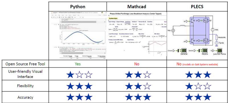
A comparison of Python, Mathcad, and PLECS for system loss analysis. An insulated metal substrate (IMS) board was used with forced air cooling. A GS66516B GaN device is the transistor candidate with RϴJA of 5.4°C/W per GaN device.
Python, Mathcad, and PLECS all have built-in temperature iteration capability. Depending on designer preferences, each tool offers different features and options. Python and Mathcad simulations have been verified with hardware designs such as, for example, the Python 48-12-V buck converter and Mathcad 3-kW full-bridge LLC. All three simulation tools have high accuracy. Python is an open-source, free tool and both Mathcad and PLECS require licenses. PLECS models on the GaN Systems website are free.
In terms of the user interface, PLECS is the most straightforward and the easiest to use of the three tools because many waveforms can be observed from the summation. The strength of Mathcad is the visualization of mathematical equations. If details are desired, such as loss calculations, Mathcad is preferred. In contrast, users must write the necessary code for Python to see the waveforms and equations. But Python is the most flexible of the three because it allows users to program any missing considerations into the model.