EDN describes how GaN is outperforming silicon in power management applications. This article describes how GaN transistors enabled CE+T’s Red Electrical Devils team to design the tour de force inverter that won Google’s Little Box Challenge. Their inverter produced a power density of 143 W/cubic inch in 14 cubic inches, outperforming the Little Box Challenge…
https://gansystems.com/wp-content/uploads/2016/08/littlebox.jpg90200LiquidWebhttps://gansystems.com/wp-content/uploads/2024/03/infineon-formerly-gan-fc-2.pngLiquidWeb2016-08-04 06:49:512023-08-08 09:00:54Google Little Box Challenge Showcases GaN Power Element
Charging levels are headed higher, and greater efficiency could make it easier to top up tomorrow’s bigger batteries without straining the grid. Researchers at the Advanced Power Electronics Lab at Kettering University, in partnership with auto electronics giant HELLA, now report that they have built a Level 2 onboard charger with an efficiency of 97%,…
https://gansystems.com/wp-content/uploads/2016/07/carged.jpg114200LiquidWebhttps://gansystems.com/wp-content/uploads/2024/03/infineon-formerly-gan-fc-2.pngLiquidWeb2016-07-28 14:32:192023-08-08 11:12:02Level 2 Onboard Charger with GaN Semiconductors Achieves Record Efficiency
Over the years, GaN power has been sarcastically described as “the technology of the future…and always will be.” While silicon carbide devices have been gaining a stronger beachhead in displacing IGBTs in higher voltage applications, the evolution of GaN as a cost-effective alternative to Si MOSFETs in applications from 200V up through 600V was, in…
https://gansystems.com/wp-content/uploads/2016/07/bodos-power.jpg72200LiquidWebhttps://gansystems.com/wp-content/uploads/2024/03/infineon-formerly-gan-fc-2.pngLiquidWeb2016-07-28 14:31:442023-06-20 08:11:21Podium Session at PCIM Europe Marks New Chapter in GaN Power Device Adoption
GaN Systems’ Di Chen explains how to test 650 V GaN transistors for your application. Our eval board is easily configured into any half-bridge-based topology, including synchronous boost and buck conversion modes, as well as pulsed switching to evaluate transistor waveforms.
https://gansystems.com/wp-content/uploads/2020/04/gs66508t-evbhb-650-v-half-bridge-evaluation-board.jpg356634LaunchSnaphttps://gansystems.com/wp-content/uploads/2024/03/infineon-formerly-gan-fc-2.pngLaunchSnap2016-06-13 13:27:142023-07-14 14:23:27Getting started with the GS66508T-EVBHB 650 V half bridge evaluation board
That GaN transistors outperform silicon-based solutions has never been more convincingly demonstrated than by CE+T’s Red Electrical Devils, who won first place in Google’s Little Box Challenge. At APEC 2016, Girvan Patterson, President of GaN Systems, describes to Design World / EEWorld’s Lee Teschler CE+T’s winning design of an uber-compact inverter using GaN transistors. The…
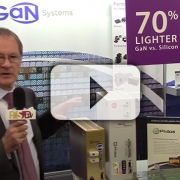
G-Philos 700W GaN-based ESS is 30% smaller, 25% less power consumption than silicon version GaN Systems President Girvan Patterson describes a 1 kV energy storage system (ESS) from Korean-based customer G-Philos that stores solar-generated power and returns unconsumed power to the grid. The GaN-based design uses both 650 V and 100 V transistors, is up…
https://gansystems.com/wp-content/uploads/2020/04/psdtv-girvan-patterson.jpg356634LaunchSnaphttps://gansystems.com/wp-content/uploads/2024/03/infineon-formerly-gan-fc-2.pngLaunchSnap2016-06-13 13:16:002023-06-20 09:48:25PSDtv – GaN Systems Shows Significant Size and Power Density Gains
The island structure is the core GaN Systems IP. It has the dual advantage of an up to four times reduction in the size and cost of gallium nitride devices, while transferring substantial current from the on-chip metal to a separate carrier. GaN Systems makes it easy for designers and systems engineers to adopt gallium…
https://gansystems.com/wp-content/uploads/2020/04/gan-island-technology.jpg356634LaunchSnaphttps://gansystems.com/wp-content/uploads/2024/03/infineon-formerly-gan-fc-2.pngLaunchSnap2016-04-13 13:32:382023-07-14 14:19:59GaN Systems – Island Technology
Gallium nitride transistors increase efficiency, lower power consumption and reduce system size and weight. GaN Systems is the first place system designers go to realize those benefits.