Improving Power Density and Efficiency in 48V Communications DC-DC Converters utilizing GaN Transistors
This article was originally published in EDN Magazine.
by Di Chen, Applications Engineering Manager, GaN Systems
Jason Xu, Applications Engineer, GaN Systems
Background
As the world’s demand for data increases seemingly out of control, a real problem occurs in the data communications systems that have to handle this traffic. Datacenters and base stations, filled with communications processing and storage handling, have already stretched their power infrastructure, cooling and energy storage to their limits. However, as the data traffic continues to grow, higher density communications and data processing boards are installed, drawing even more power. As shown in Figure 1, in 2012, communications power consumptions of networks and datacenters added up to 35% of the overall electricity use in the ICT sector. By 2017, networks and datacenters will use 50% of the electricity, and it will continue to grow.

One solution to this problem is to re-architect datacenter systems from distributing 12V power along the backplane to distributing 48V on the backplane. Just recently, in March 2016, in the USA, Google announced that it will join the Open Compute Project, and contribute its knowledge and experience (since 2012) of utilizing a 48V distributed power system. Though this helps to solve one problem, it creates another: How do the power designers of the communications and data processing cards increase the efficiency, decrease the size and increase the power levels of their DC-DC converters, provided from 48V?
In today’s architectures, using 12V backplanes, the industry is able to use 40V MOSFETs with very good Figure of Merit (FOM) characteristics to be able to switch at high frequency, deliver high efficiency and high power density. Using a 48V backplane forces DC-DC designers to use 100V MOSFETs, which have significantly higher FOM values and therefore are inherently less efficient. 100V enhancement mode GaN devices, however, are able to meet the challenges of DC-DC designers by delivering a very high efficiency, high frequency solution, as shown by comparing the FOM values in Table 1.

Table 1 shows that a 100V MOSFET increases the FOM by a factor of 2.3 and the gate drive power by a factor of 2.4 compared to the 40V MOSFETs. However, the 100V GaN E-HEMT transistor, having exceptionally good switching performance, offers a FOM even lower than the 40V MOSFET. This allows DC-DC converter architects to reach the high efficiency and high frequency requirements of 48V high-density communications processing boards.
Design of GaN 48V to 12V DC-DC Converter
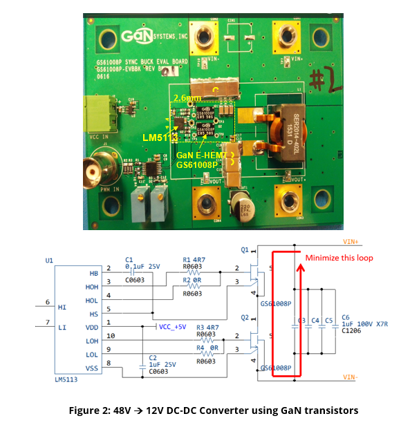
In order to compare the actual performance of GaN technology to silicon technology, the 48V to 12V DC-DC converter shown in Figure 2, using GaN transistors was created. For this test, the GS61008P from GaN Systems in Canada was used. The exceptional electrical characteristics of this device allows for both high frequency and high efficiency. The embedded packaging technique known as GaNPX® results in very low package inductance, and a very low inductive loop overall, which reduces noise, losses and improves efficiency.

Thermally, this converter uses no heat sink. The GS61008P has a very low thermal impedance of 0.55 °C/W, allowing cool operation. As recommended by GaN Systems, there are vias used underneath each of the two devices to help conduct heat to the ground plane. At an operating current of 10 amperes, at 25°C and with 500 linear feet per minute (LFM) airflow, the top and bottom device junction temperatures are 43°C and 42°C respectively.
The GS61008P GaN E-HEMT transistor operates best with a gate voltage of 0V (OFF) to 6V (ON). One specific feature of GaN Systems’ technology, with regards to gate drive, is an easy and wide tolerance gate drive level. From the data sheet, it can be seen that the gate voltage is recommended to operate from 0-6V, but is designed for a maximum voltage of 7V DC, and can tolerate spikes at the gate of up to 10V. This very easy gate drive makes the device easier to use with many gate drivers, and allows for some tolerance, ripple and noise at the gate voltage without threatening to damage the device.
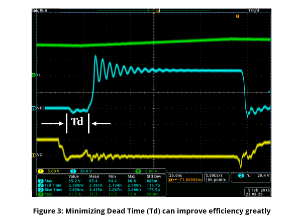
One of the most critical design considerations to make for a 48V DC-DC converter using GaN transistors is to minimize the dead time between one transistor turning off, and the other turning on. This is because in a GaN E-HEMT transistor there is no intrinsic, parasitic diode, nor is there a need for one. When the GaN transistor is forced to conduct current in the reverse direction, the reverse voltage can be as high as -2V or more. Therefore, the conduction losses during this time can be high. One might consider using a diode in parallel with the GaN transistor, but this is not required and might decrease efficiency and increase noise due to Qrr effects. Because it has no diode, the GaN E-HEMT has a higher reverse voltage. But because GaN has no Qrr (reverse recovery charge) it saves power, and possibly more importantly in communications systems, reduces noise and EMI significantly. Figure 3 shows the dead time, Td, of approximately 20ns.

In order to study the effects in efficiency of both the gate voltage, as well as the dead time, the circuit of Figure 2 was simulated so that parameters could be varied. The output power was set to 240W (12V, 20A) and the gate drive and dead time varied. Table 2 shows that the ideal (highest efficiency) operation of the GS66108P is when the gate drive is 6.0V and the dead time is 15ns or less. By adjusting the gate drive down to 5V, from 6V, the circuit dissipates 0.26W more, resulting in a slight 0.1% loss in efficiency. On the other hand, there is a more significant effect on the dead time, increasing power loss by 0.78W or reducing efficiency by 0.3%. These numbers may seem quite small, but when striving for the highest overall efficiency, working with this exceptional GaN technology, and understanding how to optimize its operation is very important.

For this design, the LM5113 GaN driver from Texas Instruments was used, even though it only supports a gate voltage of 5.0V. One feature of the LM5113 is the separate output pins HOH and HOL, allowing for a higher gate resistor in the ON direction and a lower gate resistor in the OFF direction. Because the threshold voltage of these GaN transistors are approximately 1.5V, having two different resistors helps control both the turn on and turn off waveforms perfectly. Also, using a lower turn off resistor helps to manage the Miller Effect, insuring that the lower transistor is not falsely turned on during the turn off transition periods. Another feature of this driver is the relatively short delay time of approximately 25-45ns, and it’s well-matched delay time of 8ns from the LOW side turning on to the HIGH side turning off.
Very soon, products with both higher gate drive (6.0V) and lower delay times (15nS) will be released. Once such product soon to be released from UPI Semiconductor is the uP1964. It will allow the gate drive to be optimized to 6V, has 13.5nS delay times, 5ns rise times, and will therefore provide even higher efficiency in the future. GaN transistors emerged into the marketplace in 2014 from GaN Systems, and many companies, recognizing the need for using GaN for higher efficiency have designed optimized gate drivers for use with these transistors.
Experimental Results
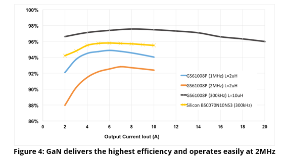
The reference design of Figure 2 was built and tested, and efficiency was measured at various operating points. Figure 4 depicts test results while operating this reference design, and also compares the efficiency at 300 kHz to a similar referenced design using a 100V Silicon MOSFET.

Figure 4 clearly shows that at 300 kHz, the efficiency of GaN is substantially higher than very highly rated 100V silicon MOSFETs. This is due to the better FOM figures, the lack of Qrr losses, and the significantly lower gate drive losses. With a 48V system using 100V devices, GaN transistors should be used for the highest efficiency.
The efficiency testing was started at 300 kHz using a 10uH Coilcraft inductor, part number SER2918H-103. The frequency was then adjusted to 1MHz, and a 2uH Coilcraft inductor approximately 5 times smaller was used. This demonstrates that a higher density DC-DC converter can be designed that still reaches very high efficiency values. Finally, the unit was tested at 2MHz, again resulting in a very highly efficient, stable design.
Conclusion
48V datacenters and communications systems will require DC-DC converter designers to learn how to maximize efficiency using 100V transistors. GaN E-HEMT transistors, when compared to Silicon MOSFETs at 100V and even at 40V, offer a significant improvement in FOM and gate drive performance, allowing designers to achieve high frequency, high power density designs at very high efficiency levels.


