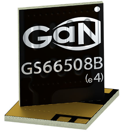
Gallium Nitride is a binary III/V direct bandgap semiconductor that is well-suited for high-power transistors capable of operating at high temperatures. Since the 1990s, it has been used commonly in light emitting diodes (LED). Gallium nitride gives off a blue light used for disc-reading in Blu-ray. Additionally, gallium nitride is used in semiconductor power devices, RF components, lasers, and photonics. In the future, we will see GaN in sensor technology.
In 2006, enhancement-mode GaN transistors, sometimes referred to as GaN FETs, started being manufactured by growing a thin layer of GaN on the AIN layer of a standard silicon wafer using metal organic chemical vapor deposition (MOCVD). The AIN layer acts as a buffer between the substrate and GaN.
This new process enabled gallium nitride transistors to be producible in the same existing factories as silicon, using almost the same manufacturing processes. By using a known process, this allows for similar, low manufacturing costs and reduces the barrier to adoption for smaller transistors with much improved performance.
To further explain, all semiconductor materials have what is called a bandgap. This is an energy range in a solid where no electrons can exist. Simply put, a bandgap is related to how well a solid material can conduct electricity. Gallium nitride has a 3.4 eV bandgap, compared to silicon’s 1.12 eV bandgap. Gallium nitride’s wider band gap means it can sustain higher voltages and higher temperatures than silicon MOSFETs. This wide bandgap enables gallium nitride to be applied to optoelectronic high-power and high-frequency devices.
The ability to operate at much higher temperatures and voltages than gallium arsenide (GaAs) transistors also makes gallium nitride ideal power amplifiers for microwave and terahertz (ThZ) devices, such as imaging and sensing, the future market mentioned above


